Welcome to Semi-Literate, a guide to the chip industry through the lens of public policy.
BLUF: The United States currently builds fewer fabs at a slower rate than the rest of the world. This post summarizes infrastructure investments and regulatory reforms that could make the United States a more attractive place to build new chipmaking capacity. The CHIPS Act aims to build more fabs in the U.S., but regulatory work at the federal, state, and local level is needed to ensure these facilities are built on time and on budget.
Introduction:
The U.S. Department of Commerce’s 100-day review of the semiconductor supply chain in response to Executive Order 14017 on Securing America’s Supply Chains found “federal incentives to build or expand semiconductor facilities are necessary to counter the significant subsidies provided by foreign allies and competitors.” However, the United States has many regulations in place which may counteract the purpose of CHIPS Act funds, slowing construction of new leading-edge fabrication facilities.
The semiconductor industry must contend with myriad environmental, health, and safety (EHS) regulations that serve important purposes, but will inevitably slow the development of a more resilient semiconductor supply chain in the United States. The simple reality is that there are very few leading-edge semiconductor manufacturers in the world, and most of them are headquartered outside the United States. In practice, this means that the United States must craft policies that convince specific foreign companies to build outside of their headquarters country, where presumably they face significant political pressure to build domestically and enjoy easier access to policymakers to facilitate build-out in regulatory environments they can navigate adeptly.
The U.S. Builds Fewer Fabs More Slowly Than the Rest of the World
It takes a long time (typically two to four years) to build a fab in any country. But fab construction takes much longer in the United States than in the East Asian countries where most chipmaking currently takes place. There are many factors underlying the decline in U.S. chipmaking capacity, but one under-appreciated factor may be the longer construction timelines associated with building new (“greenfield”) American fabs. Companies who want to build new fabs fast generally build in Asia.
In part because of the unique infrastructure requirements of fabs and the regulatory processes these large construction projects must navigate, construction of semiconductor fabs takes several years. Between 1990 and 2020 there were approximately 635 greenfield semiconductor fabs built around the world. The average time between the construction start date and the beginning date of production was 682 days or roughly 1.86 years. This timeline does not include pre-permitting and pre-construction considerations, indicating that fab construction times exceed two years on average.
Average Time it takes to Build a New Fab, by Region, 1990-2020
There is considerable regional variation in the time it takes to build a new fab. Japan (584 days) and South Korea (620 days) build fabs significantly faster than the rest of the world on average. The Americas, of which the United States is the primary site of semiconductor fabrication facilities, build fabs at a significantly reduced speed, taking an average of 736 days, or roughly five months longer than Japan. For context, in a period of five months, leading edge foundries like those operated by Samsung and TSMC could produce roughly 500,000 wafers.
From 1990-2020, the time required to build a new fab in the United States increased 38 percent, rising from an average of 665 days (1.8 years) during the 1990 to 2000 time period to 918 days (2.5 years) during the 2010-2020 time period. At the same time, the total number of new fab projects in the United States was halved, decreasing from 55 greenfield fab projects in the 1990-2000 time period to 22 greenfield fab projects between 2010 and 2020.
U.S. Average Fab Construction Time (L) and Number of Fabs by Decade (R)
The decline in the total number of new fab projects in the United States, as well as the speed with which those projects are completed, is striking when compared to other countries. In China, for example, the total number of new fab projects has increased from 14 during the 1990-2000 time period to 95 during the 2010- 2020 time period. At the same time, China has seen the average number of days from construction start date to production date for these fab projects decrease from a high of 747 days (2 years) during the 2000-2010 time period to 675 days (1.85 years) during the 2010-2020 time period. China is building more fabs and building them faster.
Chinese Average Fab Construction Time (L) and Number of Fabs by Decade (R)
How Other Government’s Facilitate Fab Construction
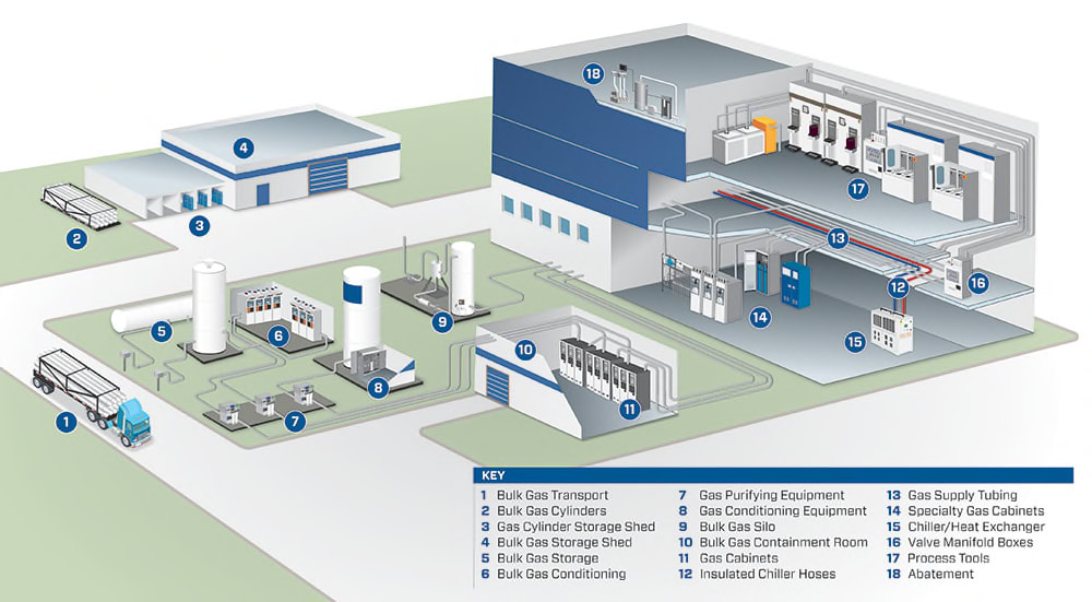
Fabs have extensive infrastructure requirements, which interact with federal, state, and local regulations in complex ways. Modern fabs require access to: (1) large plots of (2) seismically inactive land with a reliable, affordable, and stable supply of (3) water, (4) electricity, (5) talent, (6) transportation infrastructure, and (7) nearby land for co-locating with suppliers essential for constructing and operating a modern fab.

Fabs’ many infrastructure requirements implicate agencies at each level of government, sometimes with overlapping jurisdictions. As a result, construction must carefully navigate arcane regulatory processes to develop greenfield semiconductor fabs. Recognizing the time delays that these regulations and permitting processes place on semiconductor manufacturers, other countries provide incentives and indirect subsidies to expedite fab construction timelines. Below are a few country-specific snapshots:
Taiwan:
The Taiwanese government’s Ministry of Economic Affairs offers tax and tariff incentives as well as research and development (R&D) subsidies to attract semiconductor companies. Specifically, Taiwan maintains a business tax rate of 17 percent, allows semiconductor firms to credit up to 15 percent of their research & development expenses against their income tax bill annually, and permits firms to import semiconductor manufacturing equipment tariff-free. Subsidies are also available for up to 50 percent of total spending by semiconductor firms who establish an R&D center in Taiwan. International semiconductor firms are clearly responsive to these incentives. The Taiwanese government notes these incentives have successfully attracted Micron, the U.S. memory chip company, to build a fab in Taiwan, while equipment suppliers like ASML from the Netherlands, as well as Applied Materials and Lam Research from the United States, have all set up R&D centers or training headquarters in Taiwan. Taiwan’s investment authority has also helped U.S. chipmakers building fabs in-country “in terms of land acquisition…accelerated the administrative process…eliminated investment barriers (such as coordinating underground pipelines and sidewalk construction) [and] organized job fairs to help the company recruit talent.”
China:
China’s industrial plans for the semiconductor industry are well-understood, and its incentives/subsidies are clearly aimed to facilitate fab construction. Some interesting incentives that are less-visible include the provision of water and electricity to semiconductor firms at below-market rates via state utilities. Similarly, the provision of land at below-market prices to semiconductor manufacturers was observed by the OECD to be a form of investment incentive. The OECD highlighted the case of Tsinghua Unigroup, a Chinese semiconductor firm which “purchased land for its foundry in Chengdu for CNY 240 per m^2, while the official average price for industrial land in second-tier cities was CNY 724 per m^2.”
Singapore:
Through government agencies like the Economic Development Board and JTC Corporation, Singapore has established four industrial estates that provide shovel-ready plots of land for semiconductor manufacturers and their suppliers that come pre-equipped with basic infrastructure like power, electricity and roads. These estates also include ready-built facilities that feature chilled water, bulk industrial gas supply, high ceilings to accommodate SME, and incorporate vibration-control construction techniques. The results of the Singaporean government’s efforts are clear, having successfully attracted 14 global semiconductor firms employing 18,600 workers in the industry across these estates.
U.S. Regulations that Impact Fab Construction
At the federal level, there are many laws designed to maintain environmental quality that are also known to often significantly delay major construction projects. Notably, the National Environmental Policy Act (NEPA) review process governs construction projects deemed to be a “major federal action.” If the provision of CHIPS Act incentives are determined to be a “major federal action” then the construction of new semiconductor fabs could be significantly delayed. In 2020 the White House Council on Environmental Quality compiled data on timelines for 1,276 Environmental Impact Statements (EIS) filed between 2010 and 2018 and found that NEPA reviews averaged 4.5 years. This permitting process does not include the average of 1.86 years it takes to physically construct a semiconductor fab. This number also does not reflect other federal environmental reviews, some of which may happen concurrent with the NEPA process or entirely separately.
A 2017 report from the White House also identified pre-construction permits and operating permits required under the Clean Air Act as “the primary barrier to responsible and timely facility permitting” finding that “for some large projects, [this] permitting process can take 12–18 months.” More recently, the EPA has announced a goal to make permitting decisions within six months of receipt. But as discussed earlier, given the tight timelines on which this industry operates, any delay can be costly to a firm’s competitiveness.
Recent Legislation To Solve This Problem
Sens. Hagerty, King and Portman recently introduced an amendment to the NDAA that would ease the regulatory burden for technology construction projects. The amendment would add key technologies — like semiconductors or electric vehicle batteries — to the FAST-41 federal permitting program. The FAST-41 program has been in operation for several years and aims to increase coordination between permitting agencies while also maintaining the health, safety, or environmental protection intent behind may of these regulations.
However, it does not look like this amendment made it in to the recently-signed 2022 NDAA.
Conclusion
The U.S. has a substantial deficit in semiconductor manufacturing. From 1990 to 2020, China built 32 fabs that produce 100,000 or more wafer starts per month (WSpM), while the rest of the world only built 24 during the same time period. The United States had no greenfield fab projects that involved construction of factories with capacity greater than or equal to 100,000 WSpM during this 30-year time period.
Number of 100,000 WSpM Fab Projects By Region (L) and Average Construction Time (R), 1990-2020
The CHIPS Act aims to solve this problem. And the recent announcements about new U.S.-based fab construction by Samsung, TSMC, and Intel are encouraging. However, getting these fab construction projects completed on time and on budget will necessitate that regulators help clear the way.
For more information on this subject, read this recent paper from Georgetown University’s Center for Security and Emerging Technology.
The views expressed here are my own and not those of employers past or present.


